I recently released FreeFall 800, open source firmware for the Gravity 800 smoker/grill from Masterbuilt. The project started because I needed to open the controller to fix a broken wire. That is when I noticed that inside was a standard ESP32 module, with a plainly visible programming header. This made me very surprised to find that there were little to no details online about the controller’s internals. In this post I aim to document everything I managed to reverse engineer about the Gravity 800 controller board, and will discuss some of the very strange choices the designers made.
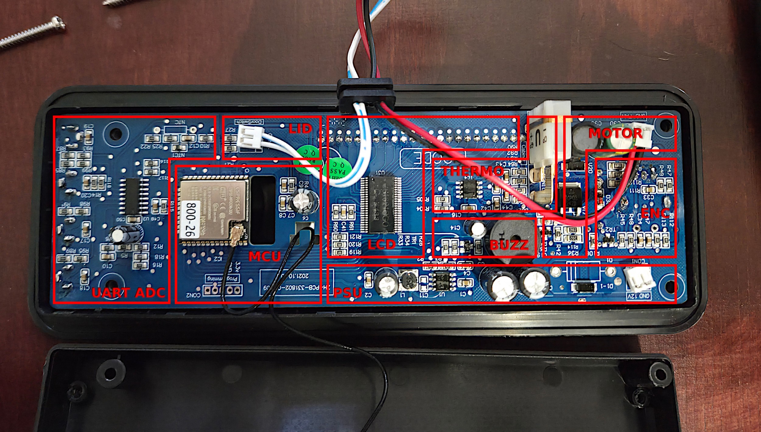
Gravity 800 Controller Board. (I apologize for the image quality in this post, I thought my phone camera was better)
At a high level the Gravity 800 controller board has the following major components:
- ESP32 WiFi microcontroller module
- Four character, 16 segment LCD display with backlight
- Five button and knob encoder physical inputs
- Piezo buzzer for temperature and timer alarms
- Grill lid open switch
- Thermocouple ADC for smoker chamber temperature, with thermistor for cold junction measurement
- Four thermistor temperature probe ADC inputs
- 12-volt blower fan motor driver
Unfortunately on first investigation, other than the MCU which is specifically an ESP32-WROOM-32UE module, and the LCD driver which appears to be a CS1621, the rest of the ICs are either unmarked or do not have specific enough markings for me to find data sheets or documentation. This meant that not only did I need to reverse the PCB connectivity to build FreeFall 800, I also ended up having to reverse engineer the serial protocols, at least enough to emulate them.
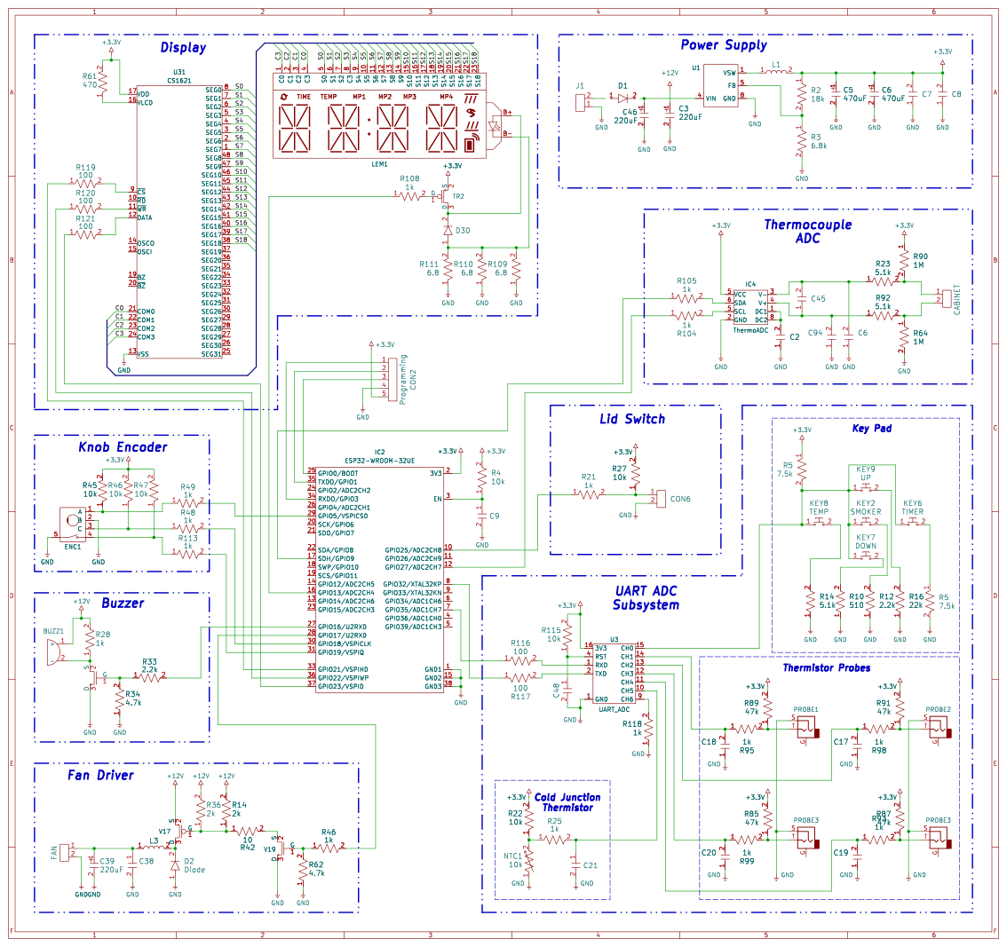
I will go through the reverse engineering process in detail below, but in the end I did end up with a full schematic of the Gravity 800 controller board. Some component values are missing (mainly unmarked capacitors and inductors, since I didn’t want to desolder them), but references should be accurate. A KiCAD project with the schematic is published in my reverse engineering repository here: prbs23/gravity-800-reverse-engineering.
Power Supply
The easiest place to start reversing the board was the power input. Not surprisingly, there does not appear to be anything too interesting going on with the power supply.
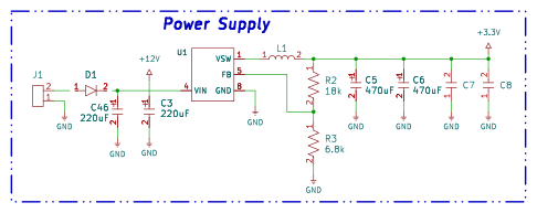
On the input side we have a reverse voltage protection diode and a couple of capacitors to produce the 12 volt rail that both feeds the 3.3 volt regulator and is used directly for the blower fan and buzzer. I was not able to identify what specific voltage regulator is being used, but it appears to be a pretty standard adjustable switching regulator configured to output 3.3V.
Microcontroller
After tracing the power supply, I moved on to the other part of the board that looked familiar: the ESP32 microcontroller. Specifically the controller uses the 8MB flash variant of the ESP32-WROOM-32UE module. In addition to the integrated WiFi and Bluetooth radios, the module has 32 GPIO that can also be used with various UART, SPI, PWM, and ADC peripherals.
Obviously the first thing to do was to connect to the programming header and dump the firmware. The programming header was conveniently labeled “Programming” and had the following pin out:
| Pin | Description |
|---|---|
| 1 | RX |
| 2 | TX |
| 3 | GPIO0/BOOT |
| 4 | GND |
| 5 | 3.3V |
Like all ESP32s the programming header does double duty as a serial debug interface while the processor is running. You can boot into the programming boot loader by tying GPIO0/BOOT low while applying power to the controller. In the first (of several) annoying decisions made by the designers, the reset (EN) of the ESP32 is simply pulled high on the board, and not exposed on the programming header. This means every time we want to program the part, it’s necessary to power cycle the board. That must have been annoying for their firmware developers.
Dumping the firmware was as simple as installing espflash and running:
espflash read-flash --port /dev/ttyUSB0 --baud 115200 --chip esp32 0 0x800000 firmware_dump.bin
There is no flash protection or encryption enabled on the controller, so I now had the full flash image. I did end up doing some basic decompilation and tracing of the firmware in Ghidra and Claude. However, other than some specific thermocouple calibration functions (discussed more later), I did not find much else in the firmware that was worth the effort of tracing in detail.
The serial debug output did not have anything particularly helpful for reverse engineering. However it does expose some details of the infrastructure the mobile app is built on top of. Once connected to a WiFi network, this is a snippet of the (hopefully anonymized) messages that were logged:
|
|
The most obvious thing we can see from this log is that they are using the AWS IoT Core managed MQTT message broker. Both from the log messages, and also some light decompiling it appears they are likely using the Espressif esp-aws-iot library for doing this. Interestingly, this trace was captured while the controller was in the “off” state. So even when “off” the controller is still sending the full device state to AWS and Masterbuilt, including your WiFi router SSID and RSSI.
Pinout
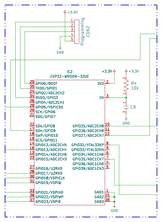
While this was interesting, it was not particularly helpful for my reverse engineering effort. The next step was tracing all the pins of the ESP32 module to find what they were connected to. This is the full list of pin connections I ended up with after fully reverse engineering:
| Pin | Name | Direction | Destination | Function |
|---|---|---|---|---|
| 25 | GPIO0 | Input | Programming Header | Boot mode |
| 34 | U0RXD | Input | Programming Header | UART RX |
| 35 | U0TXD | Output | Programming Header | UART TX |
| 10 | GPIO25 | Input | Lid switch | Lid switch (closed=low) |
| 27 | GPIO16 | Output | Buzzer | Buzzer pulse (4kHz) |
| 28 | GPIO17 | Output | Fan Driver | Fan enable (active high) |
| 30 | GPIO18 | Input | Knob Encoder | Encoder A |
| 29 | GPIO5 | Input | Knob Encoder | Encoder B |
| 31 | GPIO19 | Input | Knob Encoder | Encoder Push Button (unused) |
| 16 | GPIO13 | Output | Display Controller | Backlight Enable (active low) |
| 33 | GPIO21 | Output | Display Controller | Display CS (active low) |
| 36 | GPIO22 | Output | Display Controller | Display WR (SCK) |
| 37 | GPIO23 | Output | Display Controller | Display SDA |
| 12 | GPIO27 | Output | Thermocouple ADC | Thermocouple ADC SCK |
| 26 | GPIO4 | Bidir | Thermocouple ADC | Thermocouple ADC SDA |
| 8 | GPIO32 | Input | UART ADC | ADC UART RX |
| 7 | GPIO35 | Output | UART ADC | ADC UART TX |
One thing that I was surprised NOT to find while probing the ESP32 pins was any of the control push buttons. Given the number of free pins I was expecting them to be directly connected, but after some tracing I found that the push buttons appeared to be multiplexed, and connected to what I have been calling the UART ADC.
UART ADC Subsystem
Tracing the push buttons I ended up looking at the U3 chip on the controller, an unmarked 16-pin SOIC. This chip is connected to the ESP32, through what appeared to be a 9600 baud UART interface. While both TX and RX are connected between ICs, the ESP32 factory firmware never appears to send anything, and U3 automatically starts sending out a 16 byte message every 36 milliseconds when power is applied.
Other than power and some decoupling, the remaining pins of U3 are connected to: The four temperature probe thermistor inputs, a board mounted NTC thermistor (which I eventually determined was used for the cold thermocouple cold junction temperature), and… the push buttons for the controls. This all points towards U3 being an ADC; however, it is pretty rare for an ADC to use 9600 baud UART instead of SPI or I2C. Of the few UART ADCs I could find, none matched the description of U3. My best guess is that it’s a cheap MCU programmed to behave as an ADC for the ESP32. Why would they not just use a SPI or I2C ADC? Why not just use the ADC inputs of the ESP32?
Weird design decisions aside, I captured a couple of trace samples of the 16 byte messages the “UART ADC” was sending out:
| Byte # | 0 | 1 | 2 | 3 | 4 | 5 | 6 | 7 | 8 | 9 | 10 | 11 | 12 | 13 | 14 | 15 |
|---|---|---|---|---|---|---|---|---|---|---|---|---|---|---|---|---|
| Frame 1 | E1 | 0F | FD | 0F | FA | 0F | FB | 0F | FB | 0F | FA | 08 | 03 | 00 | 00 | 1E |
| Frame 2 | E1 | 0F | FC | 0F | FB | 0F | FB | 0F | FB | 0F | FB | 08 | 03 | 00 | 00 | 1F |
| Frame 3 | E1 | 0F | FC | 0F | FB | 0F | FC | 0F | FA | 0F | FB | 08 | 03 | 00 | 00 | 1F |
Every message starts with a 0xE1 start byte, followed by what appears to be 7 (odd?) two byte ADC sample values, and ending with a check byte. Bits [15:12] of each sample value are zero, so everything is pointing towards this being a 12 bit ADC. The check byte appears to be calculated as: check_byte = sum(frame[0:15]) % 256. This would make the frame format look something like:

The seven inputs of the ADC are mapped as follows:
| Pin | Channel | Input |
|---|---|---|
| 15 | CH0 | Multiplexed push buttons |
| 14 | CH1 | Thermistor probe 1 |
| 13 | CH2 | Thermistor probe 2 |
| 12 | CH3 | Thermistor probe 3 |
| 11 | CH4 | Thermistor probe 4 |
| 10 | CH5 | Thermocouple cold junction thermistor |
| 9 | CH6 | Unused, tied to GND |
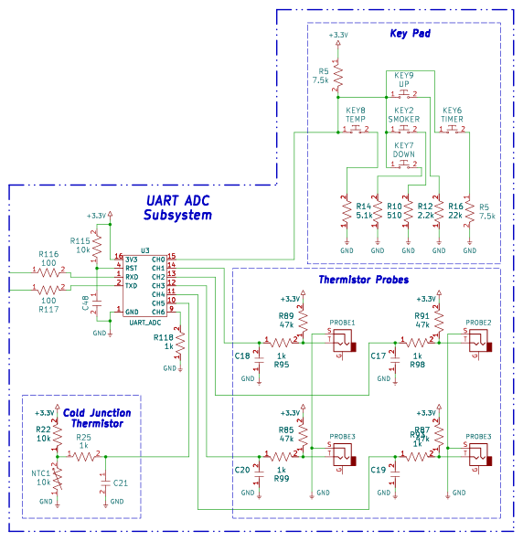
This schematic shows the whole UART ADC subsystem, with button multiplexing and thermistor conditioning.
Multiplexed Push Buttons
Despite having plenty of free IO on the ESP32, and there only being 5 push buttons on the board, the designers chose to multiplex all the buttons through a single ADC input on the UART ADC. The ADC input is pulled up with a 7.5kΩ resistor, and then all 5 buttons pull the input down with a different strength resistor. The table below lists the pull down strengths, expected output voltage, as well as ADC thresholds I ended up using.
| Button | Pulldown | Nominal Voltage | ADC Value | Positive Threshold | Negative Threshold | Window Size |
|---|---|---|---|---|---|---|
| None | N/A | 3.3V | 4095 | N/A | 3971 | 124 |
| Timer | 100kΩ | 3.069V | 3810 | 3931 | 3452 | 379 |
| Up | 22kΩ | 2.461V | 3054 | 3412 | 2375 | 1037 |
| Temp | 5.1kΩ | 1.336V | 1657 | 2335 | 1312 | 1023 |
| Enter | 2.2kΩ | 0.748V | 928 | 1272 | 624 | 648 |
| Down | 510Ω | 0.210V | 260 | 574 | 0 | 594 |
To prevent button confusion, in my FreeFall 800 firmware, I chose my thresholds such that there is a 40 ADC code window between each button’s window where I do not detect any button. Due to the structure used, detecting multiple buttons pushed at once is sort of possible, but supporting it would narrow the ADC value windows for single button presses. I have not done the math to figure out which combinations are uniquely detectable.
Thermistors
The other five (used) inputs to the UART ADC all come from NTC thermistors, which use the same structure: A voltage divider with fixed pullup and the thermistor as the pull down, followed by an RC low pass filter.
The probe inputs use a 47kΩ pull up resistor, and the thermistors have a nominal 230kΩ resistance at 25°C. From the decompiled factory firmware, it appears to use a fixed β value of 4331, so the temperature can be resolved using the following formula:
The final thermistor input is a board mounted NTC thermistor that is used as a cold junction temperature measurement for the thermocouple temperature calculation. This thermistor has a nominal 10kΩ resistance at 25°C, and uses the same input structure with a 10kΩ pull up resistor. The β value used by the factory firmware in this case is 4104. Because the same input structure is used, the same equation can be used to calculate temperature.
From my testing, the physical implementation of this cold junction thermistor has some design problems. The most obvious is that it is not located anywhere near the actual thermistor junction. A bad design decision, but not the biggest issue. The bigger problem is they used a tiny 0603 SMT thermistor, which, with a nominal 165μA passing through it, self heats to about 5-10°C above the board nominal temperature. This error then gets inferred into the thermocouple measurement, giving a constant offset.
Thermocouple ADC
Unlike the temperature probes, the Gravity 800 uses a thermocouple to measure the smoker chamber temperature. This is handled by an independent single input differential ADC IC that has the reference IC4 on the controller board. Much like the UART ADC this chip did not have any useful identifying markings, and also had a weird serial interface.
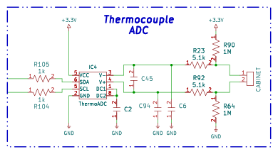
The thermocouple itself is connected to the ADC with a fairly standard 1MΩ biasing and low pass filter circuit. On first inspection, it appeared that the serial interface to the ESP32 was a unidirectional SPI-like interface, where the ESP32 would periodically clock a block of data out of the ADC. But after trying some initial testing under this hypothesis, the serial data line proved to use more complex bidirectional signaling.
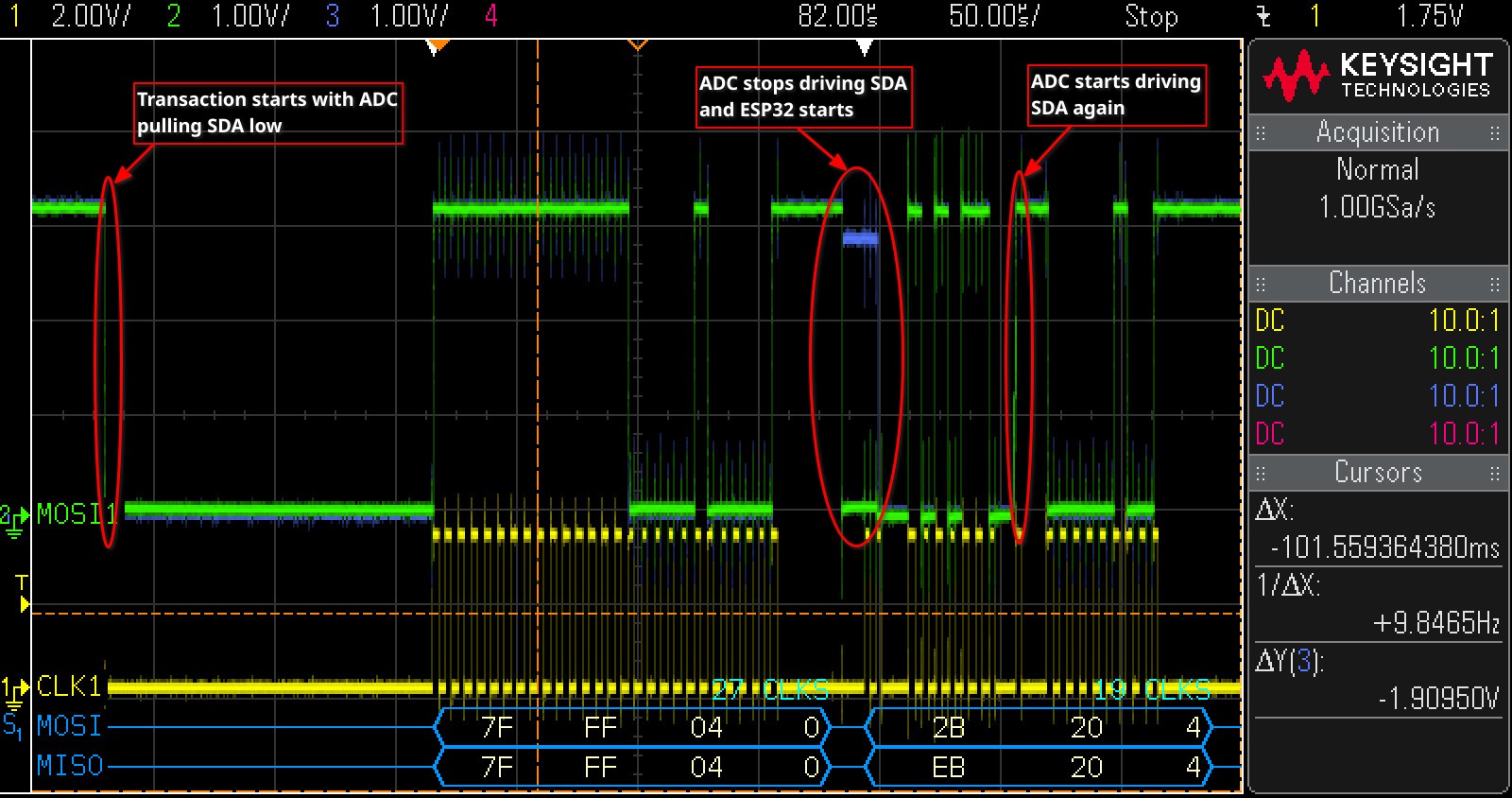
Oscilloscope trace capture of single thermocouple ADC transaction. Green trace ESP32 side of R105, blue trace ADC side of R105.
By probing the SDA signal on either side of resistor R105 and looking at the edge rate on either side, I was able to determine which side of the interface was driving SDA. From that observation the sequence appears to be:
- ADC pulls SDA low
- ESP32 sends 27 clocks, during which the ADC shifts out 27 bits of sample data
- On the next clock cycle the ADC stops driving SDA and the ESP32 starts driving
- ESP32 drives 8 clock cycle value of
0x56 - One cycle interface turn around where ESP stops and ADC starts driving SDA again.
- ESP32 clocks 9 more cycles of status data out of ADC.
- Wait for ADC to pull SDA low again.
From my analysis this is the most accurate representation of the protocol:

However, on the first transaction after coming out of reset, the factory does something slightly different. Presumably this is initializing something in the ADC. Instead of sending a fixed 0x56 command, it sends a 16 bit value of: 0xcb 0x04

Once I was able to get a 22-bit value out of the ADC, that appeared to change with temperature, I just needed to figure out how to map it to a temperature. This is where I needed to reverse engineer the factory firmware, because I had no real information on how the ADC measurements mapped to temperatures. Most of the firmware I did not fully annotate or trace, but I did identify one function which appeared to handle the calibration and correction of the thermocouple measurement.
The factory firmware appears to convert the ADC value into degrees fahrenheit with a linear scaling factor (0.00390543072717 °F/LSB), adds the cold junction temperature from the board mounted NTC, and then applies a piecewise linear correction factor. The correction function as well as a plot of its correction is shown below. Because the factory firmware does all its calculations in fahrenheit, I am showing both their coefficients in fahrenheit, and the coefficients used by FreeFall 800, which does its math in celsius.
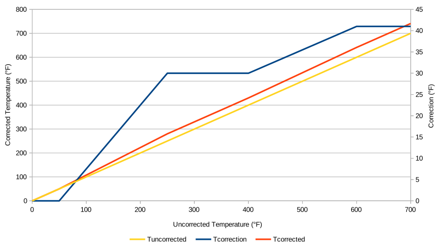
It is unclear where this correction curve comes from, it does not match any thermocouple calibration curve I was able to find. So I have to assume this is correcting for some non-linearity in the sampling circuitry, not the thermocouple itself. Additionally, since this is using a relatively coarse linear piecewise function, I suspect it is possible to get more accurate temperatures by fitting a continuous function to calibration data. However, I cannot quantify if this is worth it, since I have not yet collected the required data to test it.
This correction function is applied to the scaled and offset ADC value. The full thermocouple conversion function is shown below:
Absent better calibration and correction data, this is also temperature calculation that I implemented in FreeFall 800.
Display
The last major component of the controller board is the LCD display and controller (U31). Unlike most of the other components, I was actually able to find a datasheet for the LCD controller that matched its pin out: CS1621. The English CS1621 datasheet is missing some serial protocol details, but I found that the HT1621 appears equivalent and has a better datasheet. This made reverse engineering this part much easier than the ADCs, the main thing to figure out was the mapping of segment buffer bits to specific LCD segments.
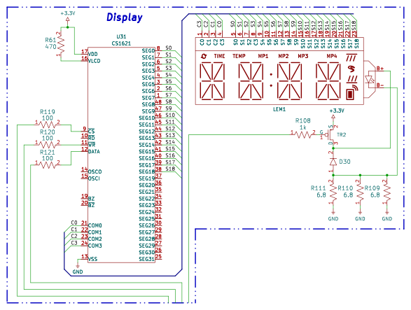
The serial interface on the CS1621 is almost SPI, and fortunately it is possible to use the SPI peripheral in the ESP32 for the way it is used on this board. Technically the interface is made up of chip select (pin 9), bidirectional serial data (pin 12), and then pins 10 and 11 are inverted read and write enables. To write a data bit to the controller the WR pin is pulled low, and then data is latched on the rising edge. To read a bit from the controller the same is done on the RD pin. However if you only need to write to the controller, you can treat the WR pin as a SPI clock signal. Since the RD pin is not connected to the ESP32, clearly this is what the designers did. (I will note they probably should have a pull up on RD, but it seems to work okay un-driven)
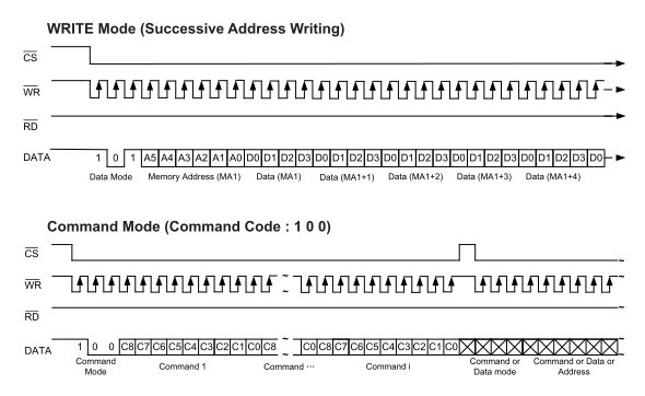
Segment Mapping
The display content is updated by using the “WRITE mode” command to update the display buffer. The factory firmware actually writes the display buffer twice in a single command, first it sends 16 bytes of 0s to clear the buffer, and then 16 bytes of actual segment state data. I am not sure this is required now that I have the datasheet, but I wrote the FreeFall 800 LCD driver before I found an English version of the datasheet so I just replicated what the factory firmware did. The table below shows the full mapping of segments:
| COM0 | COM1 | COM2 | COM3 | |
|---|---|---|---|---|
| SEG0 | CH3_E | CH3_F | CH3_H | CH3_A1 |
| SEG1 | CH3_D1 | CH3_K | CH3_G1 | CH3_I |
| SEG2 | CH3_L | CH3_G2 | CH3_J | CH3_A2 |
| SEG3 | CH2_D2 | CH2_M | CH2_C | CH2_B |
| SEG4 | CH2_L | CH2_G2 | CH2_J | CH2_A2 |
| SEG5 | CH2_D1 | CH2_K | CH2_G1 | CH2_I |
| SEG6 | CH2_E | CH2_F | CH2_H | CH2_A1 |
| SEG7 | CH3_D2 | CH3_M | CH3_C | CH3_B |
| SEG8 | CH1_E | CH1_F | CH1_H | CH1_A1 |
| SEG9 | CH1_D1 | CH1_K | CH1_G1 | CH1_I |
| SEG10 | CH1_L | CH1_G2 | CH1_J | CH1_A2 |
| SEG11 | CH1_D2 | CH1_M | CH1_C | CH1_B |
| SEG12 | CH0_E | CH0_F | CH0_H | CH0_A1 |
| SEG13 | CH0_D1 | CH0_K | CH0_G1 | CH0_I |
| SEG14 | CH0_L | CH0_G2 | CH0_J | CH0_A2 |
| SEG15 | CH0_D2 | CH0_M | CH0_C | CH0_B |
| SEG16 | BT | HT2 | SMK | HT1 |
| SEG17 | MP1 | MP2 | MP3 | MP4 |
| SEG18 | TEMP | TIME | RLD | COL |
The segment names map the the screen layout like the following:
  RLD        TIME        TEMP        MP1        MP2        MP3        MP4

 --A1-- --A2--      --A1-- --A2--         --A1-- --A2--      --A1-- --A2--     HT1
| \    |   /  |    | \    |   /  |       | \    |   /  |    | \    |   /  |
F  H   I  J   B    F  H   I  J   B  COL  F  H   I  J   B    F  H   I  J   B
|   \  | /    |    |   \  | /    |       |   \  | /    |    |   \  | /    |    SMK
 --G1-- --G2--      --G1-- --G2--         --G1-- --G2--      --G1-- --G2--
|   /  | \    |    |   /  | \    |       |   /  | \    |    |   /  | \    |
E  K   L  M   C    E  K   L  M   C  COL  E  K   L  M   C    E  K   L  M   C    HT2
| /    |   \  |    | /    |   \  |       | /    |   \  |    | /    |   \  |
 --D1-- --D2--      --D1-- --D2--         --D1--  -D2--      --D1-- --D2--     BT
.             .    .             .       .             .    .             .
+---- CH3 ----+    +---- CH2 ----+       +---- CH1 ----+    +---- CH0 ----+
Initialization and Configuration
When the controller comes out of reset it needs to be configured for the connected LCD. This is done with a sequence command of 12 bit command writes, where each command starts with a 0b100 command prefix. The configuration command sequence that the Gravity 800 factory firmware (and thus FreeFall 800) uses is:
| Command Word | Function | |
|---|---|---|
| 1. | 0x852 |
Configure bias generator for 1/3 bias voltage with 4 commons. |
| 2. | 0x830 |
Enable internal RC oscillator with 250Khz frequency. |
| 3. | 0x800 |
Disable oscillator and bias generator. |
| 4. | 0x80a |
Disable watchdog timer. |
| 5. | 0x802 |
Enable oscillator generator. |
| 6. | 0x806 |
Enable bias generator |
Backlight
The LCD backlight is driven through a high side P-channel MOSFET, connected to GPIO13 (module pin 16) of the ESP32. Because of the high side switch circuit used the backlight is enabled when GPIO13 is pulled low, and disabled when high. Annoyingly they did not include a pull up resistor on the MOSFET gate, so until the ESP32 powers on and configures GPIO13 as an output the backlight will partially turn on.
Miscellaneous
The rest of the controller is a variety of miscellaneous passive circuits
Knob Encoder
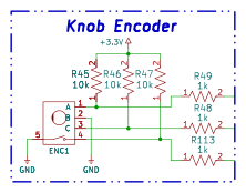
The knob is connected to a pretty standard 2 switch mechanical rotary encoder, with pull up and series resistors driving pins GPIO18 and GPIO5. Weirdly, the board has the pads and resistors to support a push button encoder, with the push button connected to GPIO19, but the actual mounted encoder is not pushable. In theory you could swap the encoder for a pushable one and have an extra user input option.
Lid Switch
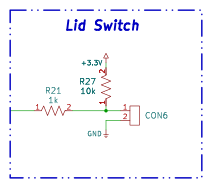
The grill lid switch uses the same pull up plus series resistor input structure for driving GPIO25.
Fan Driver
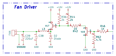
The blower fan is driven from the 12 volt supply using a high side 20P03 30V/20A P-Channel MOSFET. The gate of the 20P03 is driven from a second low side N-Channel MOSFET, so that the 3.3V ESP32 can switch the 12V motor using GPIO17. The motor output itself has a LC filter and clamp diode to protect the rest of the controller.
Buzzer
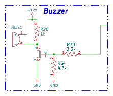
Finally, the piezo buzzer is also driven directly from the 12 volt supply, and is connected to GPIO16 of the ESP32 through a low side N-Channel MOSFET. The factory firmware always drives the buzzer with a 4kHz frequency. Presumably you could use other frequencies, but for the time being I have kept with the same configuration.
Future Work
At this point pretty much everything on the Gravity 800 controller board is fully understood. There are a few things I still want to do in this area though:
-
Reverse engineer more of the Gravity series controller boards. When I published the FreeFall 800 repository, one common piece of feedback I got was people wanting to run it on the Gravity XT controller. This is a substantially different controller with a full graphical LCD; but from the FCC filings, it appears to still use a (newer) ESP32 module. If I can get my hands on an XT, or any other model, gravity series controller I would be interested in reverse engineering them too.
-
More information on the thermocouple or UART ADCs. I have enough information to get data out of these ADCs, but if anyone has any more information about these parts, or parts with similar looking interfaces I would love to know!
-
There is still more work to do on FreeFall 800! I am currently looking into adding MQTT support, improved configuration and calibration, among other things to FreeFall 800. Additionally, in the process of writing this post and doing some deeper research into the LCD controller, I now suspect that there’s a more efficient way I could be updating the LCD.